Binary Data Storage and Manipulation
Demonstrating Physical Representation and Implementation
|
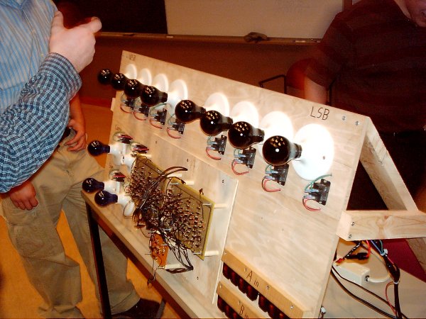
We have chosen to build an 8-bit binary adder because it is capable of working with numbers up to 255 (decimal), which we feel is a large enough value to demonstrate the significance of the project, as well as to be useful as a component of future circuitry projects. The implication of our project is incredible. We contend, that since we are able to prove by the success of our project that we can create an eight-bit binary adder from simple circuitry, that if we really wanted to and had ample time and resources to do so, that we could build an entire simple microprocessor from simple circuitry. We feel that by successfully completing this project, we will have attained much greater level of understanding of the internal workings of computers which will of course be of great benefit to us in the future. In order to build an eight-bit adder, all that is necessary is to link eight separate full-adders, the same full-adders previously described, together. On the photos of our circuit board(s), each adder is denoted by a black outline. We have used wires to interconnect the bits for simplicity, because the wires will also need to be connected to switches and lights and pin headers for the purposes of dealing with input and output. Below is the schematic that we created for a four-bit adder, which demonstrates how to interconnect full-adders to create multi-bit adders. For the sake of size and readability, we will not be creating a schematic for our eight-bit adder. The only difference between the four-bit adder and our eight-bit adder is the addition of four more bits in the middle of the schematic, a concept that can be easily imagined. 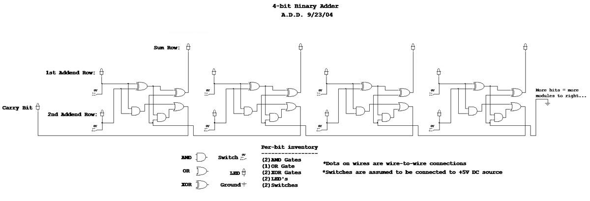 Here are some photos of our current work in progress... And yes, it really does work! :) Just click any of the photos to enlarge... 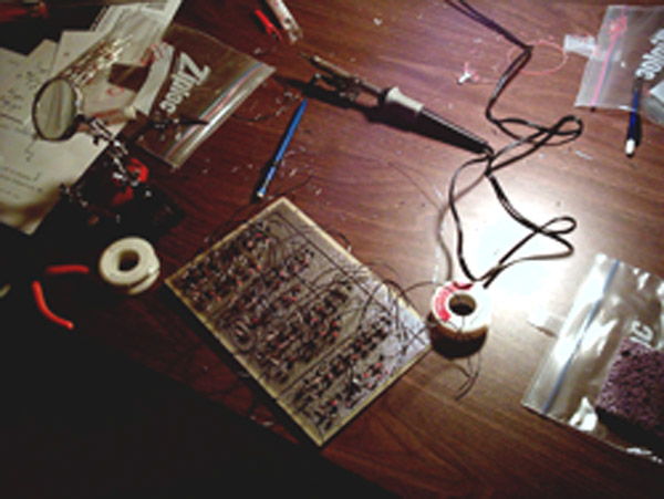 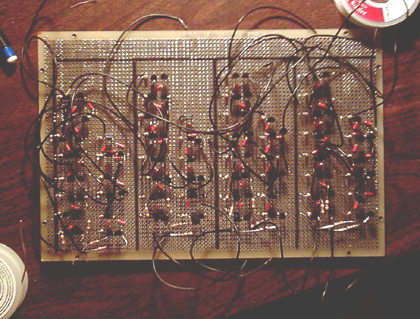 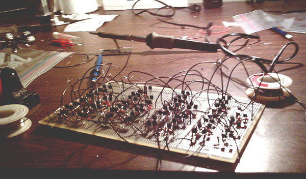
The Final Poduct: Once our two circuit boards were finished, tested, and had all of their bits interconnected, it was time to connect them to the display board. The display board uses a DC power supply, similar to the little "brick style" ones that power most common laptop computers. The display board sends input in the form of positive DC voltage to the circuit board, according to which switches have been pressed by the user. The circuit board then computes the answer by channeling the input through it's logic gates and sends the output to the relays of the display board which in turn light up the light bulbs. The relays are electronically controlled switches that allow for the switching of a dissimilar current type, in this case, the high-voltage alternating current that powers that light bulbs. 

|
(Right-Click to DL) |